Dummy OD (DOD) Rules
Must
- It is must to use TSMC’s auto-fill utilities to insert dummy OD. Don’t change any dimension and variable in utility. 必须要使用TSMC提供的自动插dummyOD的工具进行dummy的插入,并且不可以改变任何工具里的参数。
- Use the dummy layer ODBLK properly. This layer(CAD layer no. 150;20) directs TSMC utility that the area covered should be blocked from DOD, DPO fill operations. ODBLK is for excluding DOD and excluding dummy Poly(DOD).需要正确使用**ODBLK(150;20)**,这一层次会告诉TSMC工具不对这一块进行dummy插入的操作。
- Don’t put DOD in areas covered by the following marker layers:
- Well resistor under STI(NWDMY)
- Region of chip corner stress relief pattern, seal-ring, and CDU pattern
TSMC’s fill generation utility will not add DOD into these regions, as these layers are well defined. The ODBLK covered areas should not cover or overlap the above areas for DRC reasons.
DOD不能被放置在NWDMY、芯片的角上、密封环、以及CDU形状附近。
Recommended
- It is recommended to use filler cells with OD/PO to fill a large empty area in the standard-cell-based block during the P&R stage. 有标准单元(MOS管)的附近,最好采用与MOS管相同形态的Dummy对周围环境进行填充(目前我们就是这么做的),理由是TSMC的工具的填充可能会不太准确,手动插入dummy会使形状更为规整。
- It is suggested to make sure that the ODBLK layer covers sensitive circuits, such as:
- PAD areas for high frequency signals
- SRAM sensitive functional blocks and bit cell arrays
- Analog/RF circuits(DAC/ADC, PLL. Inductor) and so on…
在敏感的电路附近(模拟电路、PAD区域),要使用**ODBLK(150;20)**对层进行屏蔽处理
- It is recommended to manually add DOD uniformly inside regions covered by the ODBLK layer, to gain better process window and electrical performance. 在**ODBLK(150;20)**层次覆盖的区域,要采用手动插入dummy以保证足够的性能。
Dummy Poly (DPO) Rules
Must
- Good Poly uniformity is the key to meet the PO CD as well as circuit performance requirement. You must fill the DPO globally and uniformly even if the original drawn poly already satisfies the required poly density rule (PO.DN.1). The designer may wish to add dummy poly to improve the stability of the poly line dimension on silicon. 需要保持Poly的均一性,并且保证全局都要均一地插入DPO。
- It is must to use TSMC’s auto-fill utilities to insert dummy PO. Don’t change any dimension and variable in utility. 必须要使用TSMC的自动插Poly工具来插入dummy Poly。
- Use the dummy layer POBLK properly. This layer (CAD layer no. 150;21) directs the TSMC utility that the area covered should be blocked from DPO, DOD fill operations. POBLK is for excluding DPO and excluding dummy OD (DOD). 要使用**POBLK(150;21)**在特定区域来屏蔽DPO的填充。
- Don’t put DPO in areas covered by the following marker layers:
- Region of chip corner stress relief pattern, seal-ring, and CDU pattern
TSMC’s fill generation utility will not add DOD into these regions, as these layers are well defined. The POBLK covered areas should not cover or overlap the above areas for DRC reasons.
DOD不能被放置在NWDMY、芯片的角上、密封环、以及CDU形状附近。
Recommended
- It is recommended to use filler cells with OD/PO to fill a large empty area in the standard-cell-based block during the P&R stage. 有标准单元(MOS管)的附近,最好采用与MOS管相同形态的Dummy对周围环境进行填充(目前我们就是这么做的),理由是TSMC的工具的填充可能会不太准确,手动插入dummy会使形状更为规整。
- It is suggested to make sure that the POBLK layer covers sensitive circuits, such as:
- PAD areas for high frequency signals
- SRAM sensitive functional blocks and bit cell arrays
- Analog/RF circuits(DAC/ADC, PLL. Inductor) and so on…
在敏感的电路附近(模拟电路、PAD区域),要使用**POBLK(150;21)**对层进行屏蔽处理
- It is recommended to manually add DPO uniformly inside regions covered by the POBLK layer, to gain better process window and electrical performance. 在**POBLK(150;21)**层次覆盖的区域,要采用手动插入dummy以保证足够的性能。
Dummy Metal (DM) Rules
Must
To improve the metal CMP process window, you must fill the DMn globally and uniformly even if the originally drawn Mn has already met the density rule (Mn.DN.1/Mn.DN.2)
- Use the utility dummy fill as a method for inserting dummy metal insertion. Utility dummy fill is better for IP blocks, library cells, and full custom cells
- It is must to use TSMC’s auto-fill utilities to insert dummy metal. Don’t change any dimension and variable in utility.
需要在全局层面上插入DMn,并且保证均一性,即使我们原先的金属密度已经满足设计需求了。使用dummy fill工具作为为IP设计插入dummy 的一种方式;使用TSMC的自动插入dummy的工具在全局层面插入dummy metal。这些都是必须的
2. Use the dummy layer DMxEXCL properly. This layer directs TMSC’s utility that the area covered should be blocked from DM fill operations. All metal (geometry) beneath a customer-drawn blockage layer(DMxEXCL) must meet the density rule specified in Mn sections. 正确使用DMxEXCL层,该层次会禁止插入dummy,所有该层次下的区域都需要满足Mn层次的密度要求。
3. For DMxEXCL, use GDS layer numbers 150;n。对于屏蔽层,使用代号为150;n的层用作屏蔽。
4. 为了保证准确的RC提取操作,需要在插入dummy之后进行RC的提取,换句话说,插入dummy会引起RC数据的不精确,并且要把金属厚度是密度的函数这一特性打开。(我怀疑这里有可能就是之前我们看到金属方块电阻是金属线宽和线间距的函数的解释)
5. Don’t put DMn in areas covered by the following marker layers:
- Regions of chip corner stress relief pattern, and seal-ring.
不要在芯片角的附近以及密封环附近使用金属屏蔽层。
Recommended
- It is suggested to make sure that DMxEXCL is drawn over the following:
- Sensitive circuits & Analog circuits(DAC\ADC & PLL)
- RF application circuits
- Pad areas for high frequency signals
在敏感电路、ADC电路四周、告诉信号的PAD附近,需要使用DMxEXCL层对全部电路进行屏蔽操作,也就是说这部分的dummy是需要手动插入的。
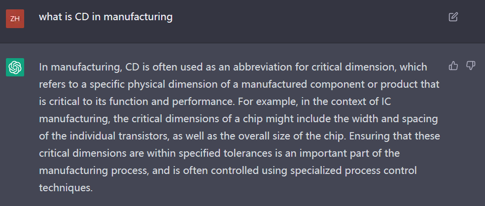
什么是process control for CD?

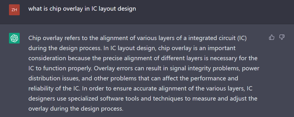
什么是 Chip Overlay?

这个链接解释了Chip Overlay是什么;由什么原因引起的;以及该如何解决?
什么是 IP abutment?


